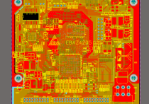
自研板卡ZYNQ7010 V2.1
板卡仿真图:

板卡实物图:
iperf3 网络测试带宽(≥500Mbits/sec):
DDR测试结果:
测试1000次大文件(500MB)读写无异常。
测试连续写入速度:126MB/s
测试连续读取速度:178MB/s
--Starting Memory Test Application--
NOTE: This application runs with D-Cache disabled.As a result, cacheline requests will not be generated
Testing memory region: ps7_ddr_0
    Memory Controller: ps7_ddr_0
         Base Address: 0x100000
                 Size: 0x3FF00000 bytes
Testing memory region: ps7_ram_1
    Memory Controller: ps7_ram_1
         Base Address: 0xFFFF0000
                 Size: 0xFE00 bytes
--Memory Test Application Complete--
Successfully ran Memory Test Application

-----------------------------------------------------------------
------------------- ZYNQ DRAM DIAGNOSTICS TEST ------------------
-----------------------------------------------------------------
 Select one of the options below:
 ## Memory Test ##
 Bus Width = 32,   XADC Temperature = 55.8995
    's' - Test 1MB length from address 0x100000
    '1' - Test 32MB length from address 0x100000
    '2' - Test 64MB length from address 0x100000
    '3' - Test 128MB length from address 0x100000
    '4' - Test 255MB length from address 0x100000
    '5' - Test 511MB length from address 0x100000
    '6' - Test 1023MB length from address 0x100000
 ## Read Data Eye Measurement Test
    'r' - Measure Read Data Eye
 ## Write Data Eye Measurement Test
    'i' - Measure Write Data Eye
    Other options for Write Eye Data Test:
         'f' - Fast Mode: Toggles Fast mode - ON/OFF
         'c' - Centre Mode: Toggles Centre mode - ON/OFF
         'e' - Vary the size of memory test for Read/Write Eye Measurement tests
 ## Data Cache Enable / Disable Option:
     'z' - D-Cache Enable / Disable
 ## Other options
     'v' - Verbose Mode ON/OFF

5Option Selected : 5


Starting Memory Test '5' - Testing 511MB length from address 0x100000...
------------------------------------------------------------------------------------------
    TEST           WORD ERROR             PER-BYTE-LANE ERROR COUNT              TIME
                     COUNT        [ LANE-0 ] [ LANE-1 ] [ LANE-2 ] [ LANE-3 ]    (sec)
------------------------------------------------------------------------------------------
................................Memtest_0 (  0: 0)      0         [       0] [       0] [       0] [       0]    17.8097
........................................Memtest_s (  0: 1)      0         [       0] [       0] [       0] [       0]    11.7098
........................................Memtest_s (  0: 2)      0         [       0] [       0] [       0] [       0]    11.7098
........................................Memtest_s (  0: 3)      0         [       0] [       0] [       0] [       0]    11.7115
........................................Memtest_s (  0: 4)      0         [       0] [       0] [       0] [       0]    11.7104
........................................Memtest_s (  0: 5)      0         [       0] [       0] [       0] [       0]    11.711
........................................Memtest_s (  0: 6)      0         [       0] [       0] [       0] [       0]    11.711
........................................Memtest_s (  0: 7)      0         [       0] [       0] [       0] [       0]    11.7098
........................................Memtest_s (  0: 8)      0         [       0] [       0] [       0] [       0]    11.7098
................................Memtest_p (  0: 9)      0         [       0] [       0] [       0] [       0]    17.424
................................Memtest_p (  0:10)      0         [       0] [       0] [       0] [       0]    17.4228
................................Memtest_l (  0:11)      0         [       0] [       0] [       0] [       0]    18.3134
................................Memtest_l (  0:12)      0         [       0] [       0] [       0] [       0]    18.3235
................................Memtest_l (  0:13)      0         [       0] [       0] [       0] [       0]    18.3134
................................Memtest_l (  0:14)      0         [       0] [       0] [       0] [       0]    18.3193
SD测试结果:
测试100次大文件(500MB)读写无异常。
测试连续写入速度:19.3MB/s
测试连续读取速度:22.1MB/s
ADC测试结果(AD7606C 8ch/16bit/1Msps):
以上测试波形为100Khz,20Vpp值的Sine波
具体的测试指标和性能待测试。